2nm Gate-All-Around Transistors: 25% Higher Density for Next-Gen Smartphone Processors
Advertisements
2nm Gate-All-Around (GAA) transistors are yielding 25% higher density for next-generation smartphone processors by enabling superior gate control and reduced leakage, leading to enhanced performance and energy efficiency.
The relentless pursuit of smaller, faster, and more efficient mobile technology has led to a groundbreaking innovation: the 2nm Gate-All-Around Transistors. This technological leap is not merely an incremental improvement; it represents a fundamental shift in semiconductor design, promising to redefine the capabilities of next-generation smartphone processors. With a remarkable 25% increase in transistor density, this new architecture is set to unlock unprecedented levels of performance and power efficiency, transforming the mobile experience as we know it.
The Evolution of Transistor Technology: From Planar to GAA
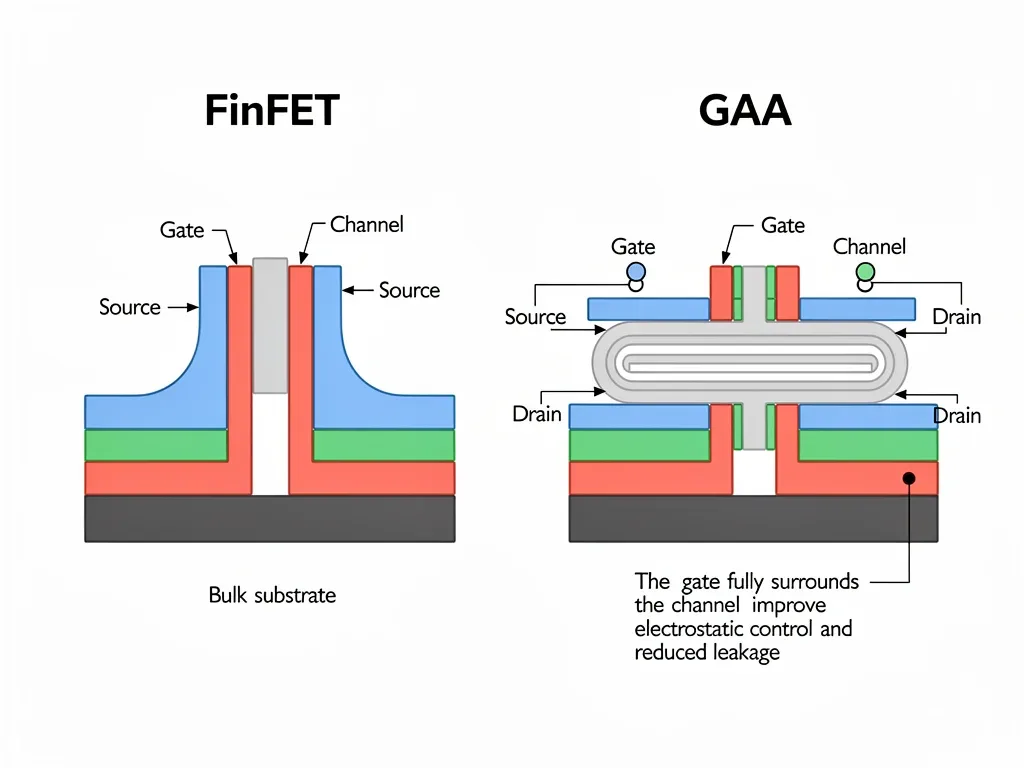
The journey of transistor technology has been one of continuous miniaturization and architectural innovation. For decades, planar transistors dominated the semiconductor landscape, but as physics dictated their limitations, a new paradigm was needed. This led to the advent of FinFETs, which offered better gate control and reduced leakage by wrapping the gate around three sides of a silicon fin.
However, even FinFETs face scaling challenges at the most advanced nodes. The desire for even greater control over the transistor channel and the need to push density further has spurred the development of Gate-All-Around (GAA) transistors. This next-generation architecture completely encircles the channel with the gate, providing optimal electrostatic control and minimizing current leakage, which is crucial for power-efficient mobile devices.
Planar Transistors: The Foundation
Early transistors were designed with a planar structure, where the gate sat on top of the channel. While revolutionary at the time, this design suffered from poor electrostatic control as transistors shrunk, leading to significant leakage currents and power consumption issues.
- Simple manufacturing process.
- Limited scalability due to short-channel effects.
- High power leakage at smaller nodes.
FinFETs: A Significant Leap Forward
FinFETs (Fin Field-Effect Transistors) addressed many of the planar transistor's shortcomings by introducing a 3D structure. The channel was elevated into a silicon fin, and the gate wrapped around three sides of this fin. This improved gate control dramatically, reducing leakage and enabling further scaling.
- Enhanced electrostatic control.
- Reduced leakage current and improved power efficiency.
- Dominant architecture for several generations of processors.
The evolution from planar to FinFET and now to GAA demonstrates the industry's relentless pursuit of physical limits. Each architectural shift has been necessitated by the fundamental challenges of scaling, aiming to pack more transistors into a smaller area while maintaining or improving performance and power efficiency. GAA is the latest answer to these challenges, setting the stage for the 2nm node and beyond.
Understanding Gate-All-Around (GAA) Architecture
Gate-All-Around (GAA) transistors represent a pivotal advancement in semiconductor technology, moving beyond the FinFET structure to achieve superior control over the transistor's channel. In GAA, the gate completely surrounds the silicon channel, hence the name, providing optimal electrostatic control from all four sides. This full encirclement is critical for mitigating short-channel effects that become increasingly problematic at smaller process nodes.
The primary advantage of GAA is its ability to significantly reduce current leakage, a persistent challenge in transistor miniaturization. By tightly controlling the flow of electrons through the channel, GAA transistors can switch more efficiently, consuming less power while maintaining high performance. This is particularly vital for smartphone processors, where battery life and thermal management are paramount concerns.

Nanosheet and Nanowire Implementations
GAA transistors can be implemented in various forms, with nanosheet and nanowire structures being the most prominent. Nanosheet GAA transistors stack multiple silicon nanosheets horizontally, allowing for flexible channel width adjustments. This flexibility is a key differentiator, enabling chip designers to optimize transistor performance for different applications, from high-performance cores to low-power cores within the same processor.
- Nanosheet GAA: Offers adjustable channel width for performance tuning.
- Nanowire GAA: Utilizes cylindrical silicon wires for even tighter gate control.
- Both aim to maximize gate control and minimize leakage.
The ability to scale down transistor dimensions without compromising performance or increasing power consumption is what makes GAA so compelling. For the 2nm node, this architecture is not just an option but a necessity to achieve the desired density and efficiency targets. The transition to GAA requires significant changes in manufacturing processes, including new etching techniques and material deposition methods, but the benefits in terms of device performance and density gains justify these investments.
The 2nm Node: Pushing the Boundaries of Miniaturization
The 2nm process node marks a significant milestone in semiconductor manufacturing, representing an unprecedented level of miniaturization. At this scale, the physical dimensions of transistors are approaching the atomic limit, making every architectural decision and manufacturing process intensely challenging. Achieving 2nm requires not only advanced lithography techniques but also a fundamental rethinking of transistor design, which is where Gate-All-Around (GAA) technology becomes indispensable.
Moving to 2nm offers several critical advantages. Firstly, it allows for an even greater packing density of transistors on a single chip. This means more computational units, more cache memory, and more specialized accelerators can be integrated into the same silicon footprint. For smartphone processors, this translates directly into enhanced multi-core performance, faster AI processing, and more sophisticated graphics capabilities, all within the strict power and thermal envelopes of mobile devices.
Challenges and Innovations at 2nm
Manufacturing at 2nm involves overcoming immense technical hurdles. Extreme Ultraviolet (EUV) lithography, already a complex process, becomes even more critical for defining such minute features. Furthermore, new materials and deposition techniques are required to construct the intricate GAA structures with atomic precision. Preventing defects at this scale is a monumental task, demanding innovative quality control and process optimization.
- Advanced EUV lithography for feature definition.
- Novel materials for optimal electrical properties.
- Sophisticated defect detection and prevention.
The 2nm node, empowered by GAA transistors, is not just about making things smaller; it's about making them smarter and more efficient. The increased transistor density directly contributes to a more powerful and responsive user experience, enabling features and applications that were previously confined to high-end computing. This technological frontier is where the future of mobile computing is being forged, promising a new era of smartphone capabilities.
25% Higher Density: Impact on Smartphone Processor Design
The 25% higher density achieved by 2nm Gate-All-Around (GAA) transistors is a game-changer for smartphone processor design. This significant increase in transistor count within the same or even smaller die area directly translates into a cascade of improvements across various aspects of mobile computing. It allows chip designers unprecedented flexibility to enhance performance, integrate more features, and optimize power consumption, leading to a new generation of highly capable smartphones.
One of the most immediate impacts is on raw computational power. With more transistors available, processor architects can design more powerful CPU cores, larger and faster on-chip caches, and more sophisticated GPU units. This means smartphones will be able to handle more demanding applications, run complex AI algorithms locally, and deliver console-quality gaming experiences, all while maintaining smooth and responsive operation.
Architectural Enhancements and Specialization
Beyond raw power, higher density enables greater specialization. Chip designers can integrate more dedicated accelerators for tasks like AI/Machine Learning, image processing, and security. These specialized units can perform specific computations far more efficiently than general-purpose CPU cores, leading to significant performance gains and power savings for common smartphone workloads.
- More powerful CPU and GPU cores.
- Larger on-chip caches for faster data access.
- Integration of specialized AI/ML accelerators.
- Enhanced security modules.
The increased density also facilitates heterogeneous computing architectures, where different types of cores and accelerators work in concert to optimize performance and power. For instance, a processor might dynamically allocate tasks to high-performance cores for intensive computations and to ultra-low-power cores for background processes, extending battery life without sacrificing responsiveness. This holistic approach to chip design, made possible by higher transistor density, is crucial for meeting the diverse demands of modern smartphone users.
Performance and Power Efficiency Gains for Mobile Devices
The transition to 2nm Gate-All-Around (GAA) transistors brings substantial improvements in both performance and power efficiency, which are critical metrics for any mobile device. The enhanced electrostatic control offered by the GAA architecture directly translates into faster switching speeds and reduced leakage currents. This means transistors can operate more quickly, completing computations in less time, while simultaneously consuming less power during both active and idle states.
For smartphone users, these improvements manifest as a noticeably snappier and more responsive device. Applications launch faster, multitasking becomes smoother, and graphically intensive games run at higher frame rates with greater stability. More importantly, these performance gains come without the typical trade-off of increased battery drain. Instead, the inherent power efficiency of 2nm GAA transistors helps extend battery life, allowing users to do more on a single charge.
Optimized Battery Life and Thermal Management
Reduced power consumption is a direct benefit of GAA's superior leakage control. Less leakage means less wasted energy, which directly extends the operational time of a smartphone. Furthermore, lower power dissipation also leads to less heat generation. This is a significant advantage for thermal management within the compact confines of a smartphone, preventing overheating and allowing the processor to sustain peak performance for longer periods without throttling.
- Faster application loading and execution.
- Smoother multitasking capabilities.
- Extended battery life through reduced power consumption.
- Improved thermal performance, preventing overheating.
These gains are not just theoretical; they are fundamental to enabling the next generation of mobile experiences. From always-on AI assistants that continuously process data with minimal battery impact, to immersive augmented reality applications that demand immense computational resources, the performance and power efficiency of 2nm GAA processors are the bedrock upon which these innovations will be built. The ability to deliver high performance in a power-constrained environment is what truly sets this technology apart.

Future Implications and Market Impact
The introduction of 2nm Gate-All-Around (GAA) transistors is set to have profound implications for the semiconductor industry and the broader technology market, especially concerning future smartphone development. This technological leap will not only redefine the capabilities of mobile devices but also influence innovation in related fields, from edge computing to artificial intelligence. The market impact will be substantial, driving new product cycles and fostering intense competition among chip manufacturers and smartphone brands.
One of the most significant implications is the accelerated development of advanced mobile AI. With dramatically increased processing power and efficiency, future smartphones will be able to perform highly complex AI computations locally, reducing reliance on cloud-based services. This will lead to more personalized, responsive, and secure AI experiences, from sophisticated voice assistants to real-time language translation and advanced computational photography.
New Frontiers in Mobile Technology
Beyond AI, 2nm GAA processors will enable new frontiers in mobile gaming, augmented reality (AR), and virtual reality (VR). The ability to render highly detailed graphics and complex environments with low latency and extended battery life will transform how users interact with digital content. Furthermore, the enhanced processing capabilities will support the proliferation of advanced sensors and connectivity options, paving the way for truly intelligent and interconnected mobile ecosystems.
- Accelerated on-device AI and machine learning.
- Enhanced mobile gaming and immersive AR/VR experiences.
- Improved capabilities for advanced sensors and connectivity.
- Driving innovation across the mobile technology ecosystem.
The market will likely see a new wave of flagship smartphones boasting unprecedented performance benchmarks and novel features, creating strong demand. Chip manufacturers that successfully master 2nm GAA production will gain a significant competitive edge, while smartphone brands that effectively leverage these new processors will be able to differentiate their products. This innovation cycle is crucial for maintaining the rapid pace of technological advancement that consumers have come to expect.
Challenges in Adopting 2nm GAA Technology
While the benefits of 2nm Gate-All-Around (GAA) transistors are undeniable, the adoption of this cutting-edge technology is not without significant challenges. The transition from established FinFET architectures to GAA requires substantial investments in research and development, as well as a complete overhaul of existing manufacturing processes. These hurdles can slow down widespread adoption and increase initial production costs, posing a barrier for some manufacturers.
One of the primary challenges lies in the complexity of manufacturing these incredibly small and intricate structures. Building nanosheets or nanowires with atomic precision, layering them, and then wrapping them with gates demands state-of-the-art lithography, etching, and deposition techniques. Even minor variations in the manufacturing process can lead to defects, significantly impacting yield rates and increasing costs.
Cost, Complexity, and Yield Rates
The cost associated with developing and implementing 2nm GAA technology is astronomical. This includes the expense of new equipment, materials, and the extensive R&D required to refine the process. These costs are ultimately passed on to consumers, making devices featuring these advanced chips more expensive initially.
- High R&D and manufacturing investment.
- Increased process complexity and precision requirements.
- Potential for lower initial yield rates.
- Need for new materials and metrology techniques.
Another challenge is the need for new metrology and inspection techniques capable of verifying the quality and integrity of 2nm structures. Traditional methods may not be sufficient to detect defects at this scale, requiring innovative solutions to ensure reliable mass production. Despite these challenges, the industry's commitment to continuous innovation means that these hurdles will likely be overcome, albeit with considerable effort and investment. The long-term benefits in performance and efficiency are too significant to ignore, ensuring that 2nm GAA technology will eventually become the standard for high-end mobile processors.
| Key Aspect | Description |
|---|---|
| GAA Architecture | Gate-All-Around transistors encircle the channel, offering superior electrostatic control and reduced leakage compared to FinFETs. |
| 2nm Node Density | Achieves 25% higher transistor density, allowing more components in a smaller area for enhanced performance. |
| Performance Boost | Faster processing, improved AI capabilities, and enhanced graphics for next-gen smartphone experiences. |
| Power Efficiency | Significantly reduces power consumption and heat generation, extending battery life and improving thermal management. |
Frequently Asked Questions about 2nm GAA Transistors
What exactly are Gate-All-Around (GAA) transistors?▼Gate-All-Around (GAA) transistors are a new type of transistor architecture where the gate completely surrounds the semiconductor channel. This design provides superior electrostatic control over the channel, significantly reducing current leakage and improving switching efficiency compared to previous FinFET designs.
How does 2nm GAA technology increase transistor density by 25%?▼The 2nm process node combined with GAA's compact design allows for a much tighter packing of transistors. By effectively controlling the channel and minimizing leakage at these ultra-small dimensions, more functional transistors can be integrated into a given chip area, leading to a 25% higher density.
What are the main benefits of 2nm GAA for smartphone processors?▼The primary benefits include significantly enhanced performance, greater power efficiency leading to extended battery life, and improved thermal management. These advancements enable faster app loading, smoother multitasking, more powerful AI processing, and better graphics for mobile gaming and AR/VR experiences.
When can we expect to see smartphones with 2nm GAA processors?▼Leading semiconductor manufacturers are targeting mass production of 2nm GAA chips in the coming years. Consumers can anticipate seeing these advanced processors in flagship smartphones likely within the next two to three years, as the technology matures and yields improve for high-volume manufacturing.
What challenges does the adoption of 2nm GAA technology face?▼Key challenges include the immense cost of research and development, the complexity of manufacturing at such small scales, the need for new materials and sophisticated metrology techniques, and managing initial low yield rates. These factors contribute to higher production costs and a demanding transition period for the industry.
Conclusion
The advent of 2nm Gate-All-Around (GAA) transistors marks a monumental leap in semiconductor technology, promising to revolutionize next-generation smartphone processors. By delivering a remarkable 25% higher transistor density, GAA architecture not only pushes the boundaries of miniaturization but also unlocks unprecedented levels of performance, power efficiency, and functional integration. While significant challenges in manufacturing and cost remain, the profound benefits for mobile computing – from enhanced AI capabilities to immersive AR/VR experiences and extended battery life – firmly establish 2nm GAA as the cornerstone of future smartphone innovation. This technological evolution underscores the industry's relentless drive to deliver smarter, faster, and more efficient mobile devices to consumers worldwide.
